Real-Time PCB Defect Detection System using YOLOv8 and Raspberry Pi
Team: Potturi Lakshmi Sri Sai Lokesh, Rohith V, Kalaiyarasan V, Naman Thakur
Code: GitHub Repository
1. Abstract
This project presents a real-time Printed Circuit Board (PCB) defect detection system using the YOLOv8 object detection model deployed on a Raspberry Pi. The system aims to automate defect inspection in PCBs, reducing human error and improving efficiency. A conveyor mechanism simulates an industrial setup, where PCBs move continuously and images are captured using a mobile device via IP Webcam. The captured images are processed using a trained YOLOv8 TFLite model to detect defects such as missing holes, mouse bites, open circuits, shorts, spurs, and spurious copper. The system outputs labeled images indicating defect presence or absence. The solution demonstrates a low-cost, scalable, and efficient approach to real-time industrial inspection.
2. Introduction
Printed Circuit Boards (PCBs) are fundamental components in electronic devices. Ensuring their quality is critical, as defects can lead to device malfunction or failure. Common PCB defects include missing holes, mouse bites, open circuits, shorts, spurs, and spurious copper.
Traditional inspection methods rely on manual visual inspection, which is:
- Time-consuming
- Error-prone
- Not scalable for large-scale production
With advancements in computer vision and deep learning, automated inspection systems have become viable. Object detection models like YOLO (You Only Look Once) enable real-time detection with high accuracy, making them suitable for industrial applications.
3. Problem Statement
Manual inspection of PCBs is inefficient and unreliable, especially in high-speed production environments. There is a need for an automated system that can:
- Detect multiple types of defects
- Operate in real-time
- Provide consistent and accurate results
- Be cost-effective and deployable on edge devices
4. Objectives
- Develop an automated PCB defect detection system
- Train a YOLOv8 model for multi-class defect detection
- Deploy the trained model on a Raspberry Pi
- Simulate real-world conditions using a conveyor system
- Achieve near real-time detection performance
- Provide visual output indicating defect presence
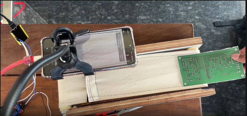
5. System Overview
The system follows the pipeline: Camera → Image Capture → Raspberry Pi → YOLOv8 Model → Output
- Images are captured using a mobile phone via IP Webcam
- The Raspberry Pi receives the image over a local network
- The YOLOv8 TFLite model performs inference
- Output is displayed and saved
6. Hardware Components
- Raspberry Pi (Edge computing device)
- Mobile phone (used as camera via IP Webcam)
- Conveyor system (for real-world simulation)
- 12v Johnson gear motor (for Conveyor system)
- L298N Motor driver Ic (for Conveyor system)
- ESP32 Dev module (for Conveyor system)
- 12v dc adapter power supply (for Conveyor system)
- 12v dc motor speed controller (for Conveyor system)
- Lighting setup (for consistent image quality) (for Conveyor system)
7. Software and Tools Used
- Python
- Ultralytics YOLOv8
- OpenCV
- TensorFlow Lite (TFLite)
- IP Webcam (Android application)
- Google Colab (for training and experimentation)
8. Dataset Description
-Dataset downloaded from Kaggle (link:- https://www.kaggle.com/datasets/akhatova/pcb-defects)
- PCB defect dataset containing annotated images
- Annotations provided in XML format (Pascal VOC)
- Classes included:
- Missing hole
- Mouse bite
- Open circuit
- Short
- Spur
- Spurious copper
- Dataset converted from XML to YOLO format
- Split into:
- Training set
- Validation set
- Test set
9. Data Preprocessing
- Converted XML annotations to YOLO format
- Verified dataset integrity (image-label matching)
- Created YAML configuration file specifying:
- Dataset paths
- Class names
- Number of classes
10. Data Augmentation
To improve generalization and handle limited data, the following augmentations were applied:
- HSV augmentation (brightness, contrast, color variation)
- Rotation (±10 degrees)
- Translation (object shifting)
- Scaling (zoom in/out)
- Horizontal and vertical flipping
- Mosaic augmentation (combining multiple images)
- Mixup augmentation (blending images)
These augmentations increase data diversity.
11. Model Training
- Model used: YOLOv8n (lightweight version)
- Training parameters:
- Epochs: 50
- Batch size: 16
- Image size: 800
- Performance metrics:
- Precision
- Recall
- mAP@50
- mAP@50-95
The model achieved strong detection performance across multiple defect classes.
12. Model Optimization
Pruning
- Applied 30% L1 unstructured pruning
- Removed low-magnitude weights
Purpose
- Improve computational efficiency
- Reduce model complexity
Limitations
- No significant reduction in file size (45MB to ~41MB)
- latency improvement on CPU
Future Need
- Quantization (INT8) required without effecting accuracy:
- Size reduction
- Faster inference
13. Deployment on Raspberry Pi
- Model exported to TFLite format
- Loaded using Ultralytics YOLO API
- Image captured via IP Webcam over HTTP
- Inference performed on Raspberry Pi CPU
Pipeline: IP Webcam → HTTP Request → Image Decode → YOLO Inference → Output
14. Working of the System
- Conveyor moves PCB
- Mobile camera captures image
- Image sent to Raspberry Pi via network
- YOLOv8 model performs defect detection
- Output is displayed and saved
- If defect detected → bounding boxes shown
- If no defect → labeled as “No defect”
15. Results
- Successful detection of PCB defects
- Accurate classification of multiple defect types
- Output with annotations
16. Performance Analysis
- Average inference time: ~1.1 seconds
- Pruning impact:
- Minimal latency improvement (~30%)
- Bottlenecks:
- Network latency (IP Webcam)
- Fixed delay in processing loop
17. Advantages
- Real-time defect detection
- Low-cost implementation
- Deployable on edge devices
- Scalable to industrial applications
- Reduces human inspection effort
18. Limitations
- Latency due to CPU-based inference
- Dependent on lighting and image quality
- Limited dataset size affects generalization
- Network dependency for image capture
19. Future Scope
- Integrate alert system (buzzer/email)
- Use industrial cameras instead of mobile
- Scale to full production environments
20. Conclusion
The project successfully demonstrates a real-time PCB defect detection system using YOLOv8 and Raspberry Pi. The integration of deep learning with edge computing enables automated inspection with reasonable accuracy and speed. Although pruning provided limited performance gains, the system establishes a strong foundation for further optimization using quantization and hardware improvements. This approach can significantly enhance quality control processes in industrial manufacturing.